Preparing secure environments
Technology Leader in Bond Testing Worldwide
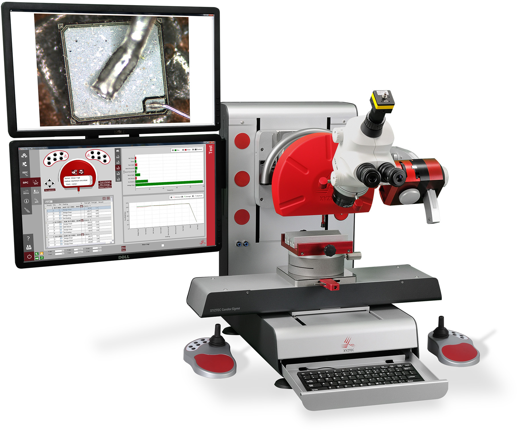
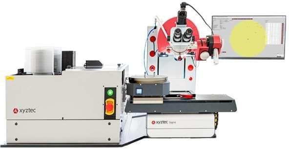
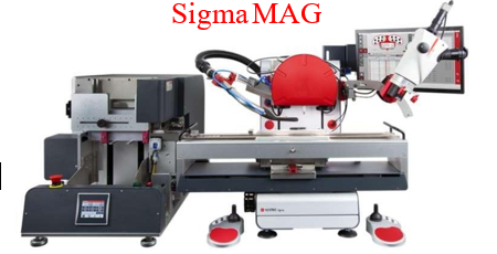
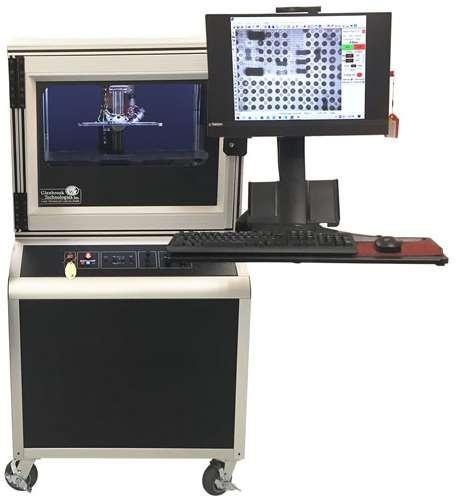
With 15+ years in-house experience, XYZTEC takes bond testing to a new level with the Condor Sigma. It combines the unique strengths of the Condor series with the latest technologies and innovations to set the new standard worldwide.
Whether you need a dedicated or multipurpose bond tester, it features unparalleled 0.075% accuracy, the best ergonomics, highest throughput, and the lowest cost of ownership.
The Sigma RMU raises new standards with the capability to be configured with up to 6 sensors in any combination of pull or shear, ranging from 10gf to 200kgf. Sensors are permanently fixed, requiring no warm-up time.
Use your existing stock of work holders and tooling with our shuffle plate. Compatibility modes ensure consistency in measurement results across machines.
Supports up to three live camera views at the same time. Features programmable landing forces and the most precise step-back accuracy in the industry.
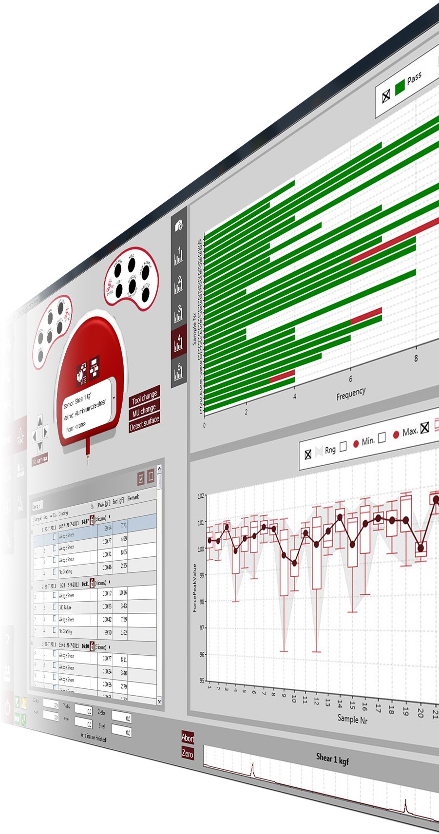
The Condor Sigma software supports various authorization levels, featuring an easy-to-learn operator screen. Engineers get full control of the production process through powerful statistical process control (SPC) and clear graphs.
| Category | Features & Capabilities |
|---|---|
| Force Sensors | Revolving (up to 6 sensors) or Single (1 sensor). Ranges: 10gf to 200kgf. ±0.075% Accuracy, 24-bit resolution. |
| Stages & Axis | 30nm resolution built-in linear encoders. Travel: X=370mm, Y=168mm, Z=168mm. Speed up to 50mm/s. |
| Supported Tests | Wire pull, Ball shear, Die shear, Solder ball shear, Ribbon pull, Copper pillar, Stud pull, Creep/Fatigue tests, and more. |
| Frame & Size | Footprint: 620mm (X) x 558mm (Y) x 608mm (H). Weight: 75-85 kg. |
| Controls | Ergonomic layout to SEMI S8. Two joysticks with 6 buttons each. Microscope moves in focal arc. |
| Services | Electric 110-240V, single phase. No compressed air required. |
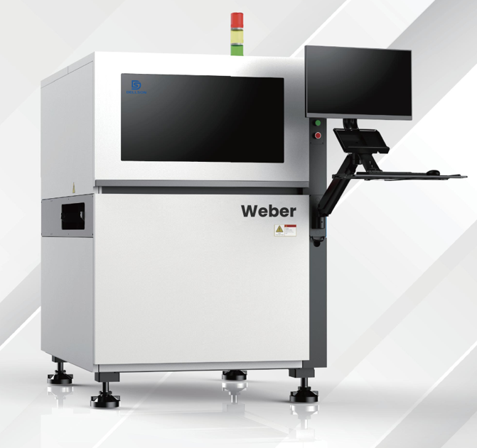
Internationally Leading Supplier of Deep Learning AOI Systems
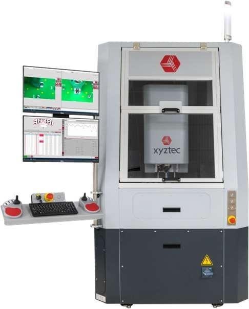
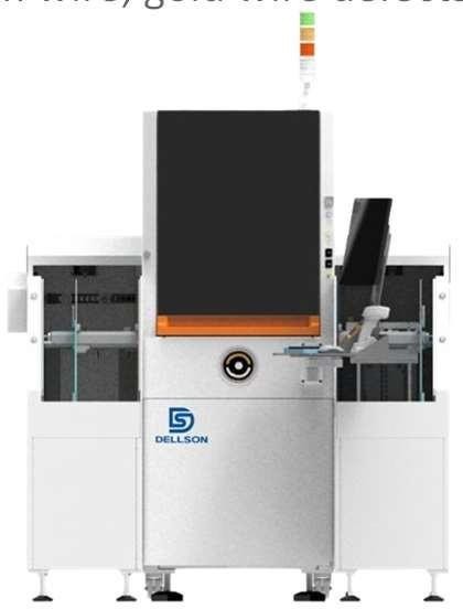
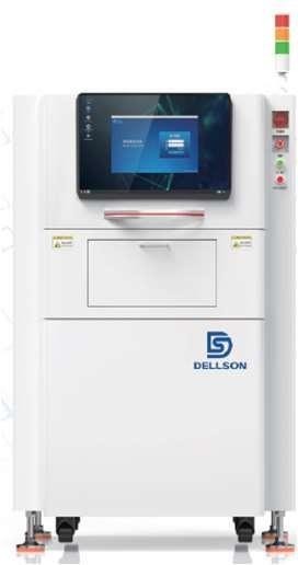
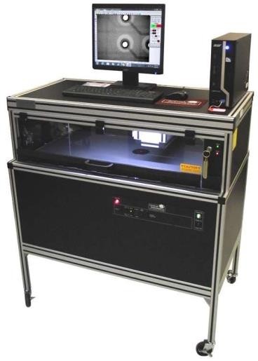
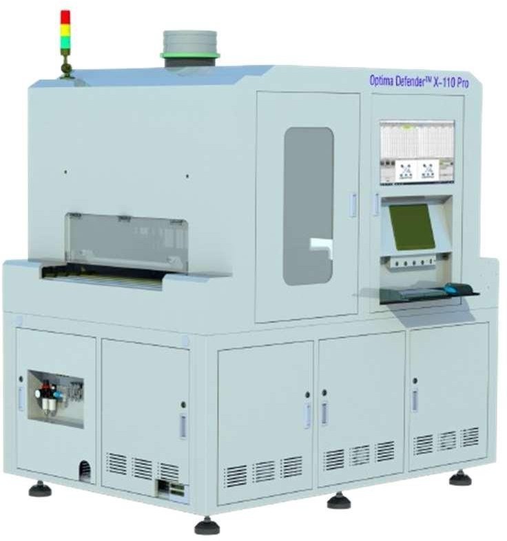
This equipment is mainly applied to detect various defects on the Die surface, die bonding, wire bonding, and lead frame surfaces during the semiconductor die attachment and wire bonding manufacturing processes. It fully supports the automated optical inspection of gold wires after module component bonding.
The core gold wire detection parameters include: gold wire count, wire shifting, bonding point shifting, and abnormal wire morphology profiles.
Features complete Wire Bonding (WB) 3D imaging capabilities. It utilizes a multi-layer focusing function and an infinite depth of field to deliver exceptionally clear imaging across the entire processing board.
Integrates an industry-exclusive zero-negative sample AI detection framework. Powered by deep neural networks trained with extensive datasets, it achieves complex appearance and structure defect detection.
Built with a high-density marble platform to ensure structural assurance for high-precision imaging. Multi-angle light sources combined with high-resolution industrial cameras and telecentric lenses vastly enhance defect visibility.
Equipped with the latest self-developed AAM absolute precision measurement system. This enables the machine to accurately pinpoint and detect both wire aluminum trace and wire bonding process variations.
Engineers gain deep process control through the AI Big Data Training Center, providing robust tracking from raw products to final analytics. The software features an offline programming mode to maximize machine uptime.
| Category | Features & Capabilities |
|---|---|
| Vision System | 12MP Industrial Camera (21MP optional). 2.7μm resolution. FOV Size: 11*8.5mm. Minimum detectable defect: 5.4μm. RGBW LED illumination. |
| Motion Mechanism | AC Servo Motor for XY movement with ±1μm accuracy. Customizable flow direction. Z-axis travel range: ≤30mm. Track height: 900±30mm. |
| Hardware & Size | Power: 200V-230V AC 50/60Hz. Power rating: 2.2KW. Air pressure requirement: 0.4-0.6MPa. Machine Weight: 1100kg. Dimensions: W1156 * D1475 * H1650 mm. |
| Inspection Criteria | Substrate Size: 50*50mm to 510*460mm. Substrate Thickness: 0.6-6mm. Measurement Height: Clear imaging for components >10mm. |
| Detected Items | Substrate defects, component faults, gold wire lifting, bending, missing wires, wire breakage, die contamination/dirt, structural damage, and surface scratches. |
| Environment | Operating Temperature: 20°C ~ 25°C. Humidity Requirements: 45%RH ~ 65%RH (Strictly non-condensing). |
Technology Leader in Plasma Cleaning, Etching, and Surface Treatment Worldwide
Founded in January 2000, SCI Automation provides advanced, highly effective plasma cleaning and surface treatment solutions engineered for the Semiconductor, Electronic, Automotive, Medical, and Life Science industries. Our high-reliability systems are fully built in Singapore and deployed globally.
Through an extensive network of highly trained engineers and localized branches, SCI guarantees excellent product quality, full technical traceability, and dependable 24/7 after-sales service support.
A standalone strip plasma system that builds upon a legacy framework first deployed in 2004 across major semiconductor factories. Equipped with completely redesigned PC controller software and updated hardware, it delivers exceptionally repeatable, consistent plasma operations and comprehensive data tracking for total process traceability.
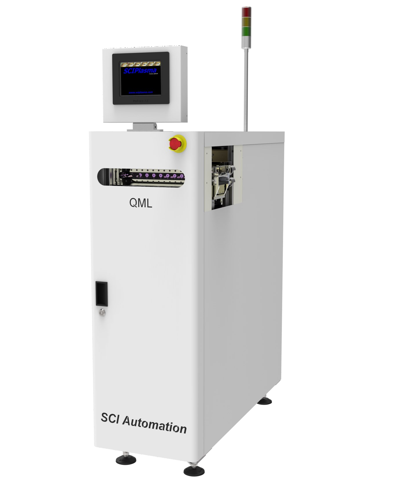
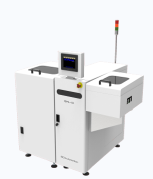
Engineered explicitly to handle strip form factor substrates directly inline. It interfaces seamlessly with upstream and downstream assembly mechanisms via the SMEMA protocol. Recognized as the smallest inline system on the market, it ensures reliable and repeatable cycling for continuous 24/7 runtime.
A compact inline system that delivers the exact high-performance plasma cleaning capabilities of the standard QML unit. It offers enhanced flexibility to process carriers, Auer boats, and ceramic substrates, featuring a dedicated conveyor belt and indexer system for fully automated assembly integration.
SCI Automation systems deliver excellent surface modification capabilities crucial for high-yield packaging operations. Key process applications include:
| Category | Features & Capabilities |
|---|---|
| Core Solutions | Quadrioα (Standalone Strip), QML (Smallest Inline Strip System), and QML-CI (Inline Boat/Ceramic Carrier System). |
| Interface Protocol | SMEMA protocol fully integrated on inline equipment for seamless automated upstream and downstream machine handshakes. |
| Material Handling | Supports strip form factors, industry-standard boats, Auer boats, and advanced ceramic substrate arrays. |
| Traceability | Completely redesigned software architecture and PC control interfaces built for strict process parameter logging and verification. |
| Global Support | Intensively factory-trained service teams with localized spare parts hubs ready for rapid global shipment and deployment. |
Advanced In-Line 2D Automated X-Ray Inspection (AXI) System
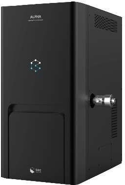
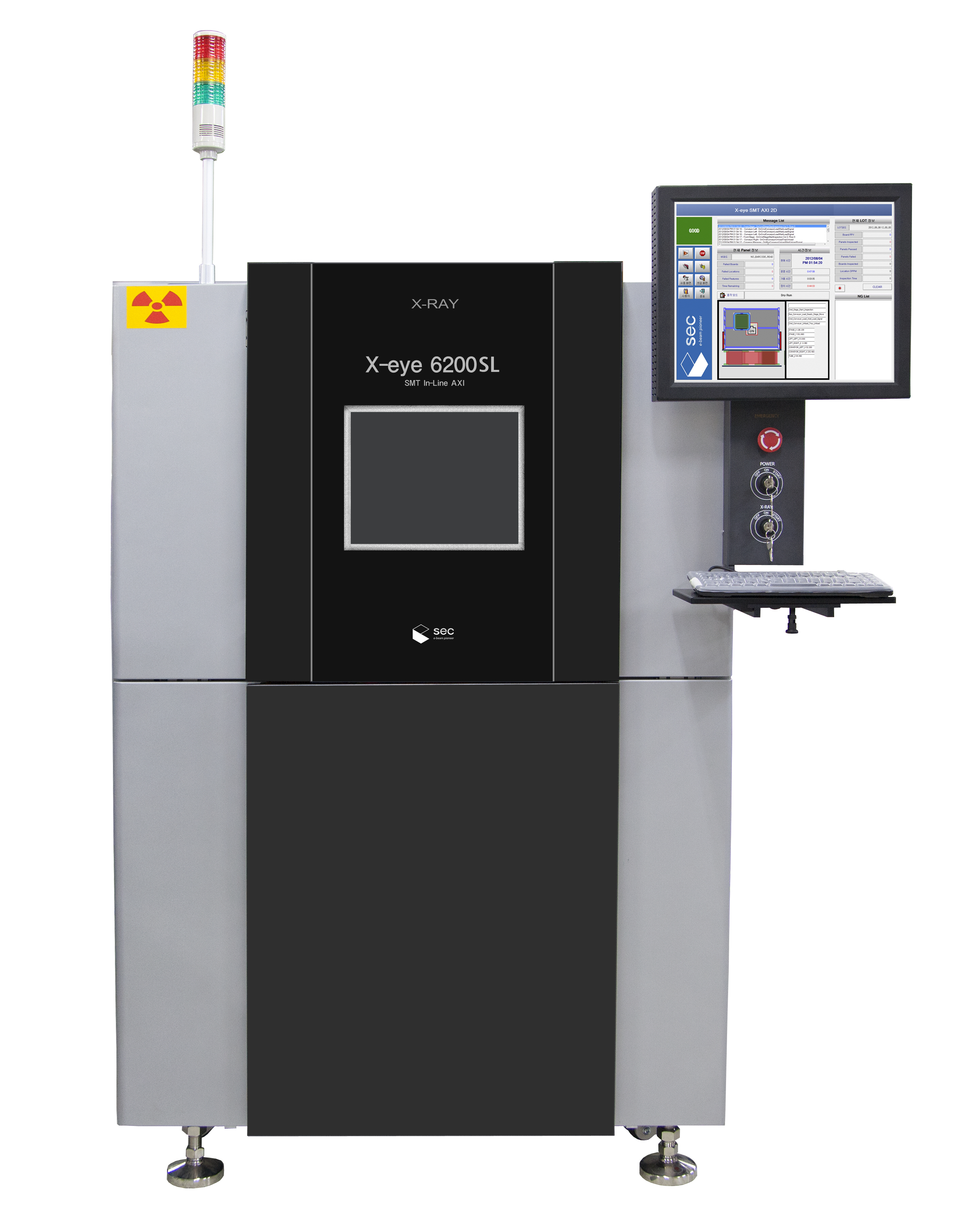
The X-EYE 6200 is an advanced In-Line 2D Automated X-Ray Inspection (AXI) System manufactured by SEC (South Korea). It is designed for high-speed, non-destructive inspection of electronic components and printed circuit board assemblies (PCBAs) during production. The system automatically detects hidden defects that cannot be seen through ordinary visual inspection.
Utilizing high-resolution X-ray imaging technology, the system inspects solder joints, semiconductor packages, wire bonding, and other electronic assemblies. It is integrated directly into production lines, allowing real-time quality control and defect detection without interrupting manufacturing processes.
The diagram shows the internal inspection cycle of the X-EYE 6200. High-intensity X-rays are emitted downward from the 160 kV tube passing through the PCBA assembly components transiting live over the automated line conveyor belt.
The ultra-precise 1.6 MP Flat Panel Detector underneath captures dense structural projections instantly. In a fraction of a second (0.5–1s per field of view), the internal core execution algorithm maps and verifies the layout, tracking out wire paths and automated classification metrics.
| Specification Key | System Equipment Details |
|---|---|
| X-Ray Tube | 160 kV / 500 µA Open-Type Hybrid Tube Configuration |
| Detector Type | 1.6 MP High-Speed Digital Flat Panel Detector (FPD) |
| Spatial Resolution | 0.8 µm to 15 µm software scalable focal depth range |
| Inspection Methods | In-Line 2D AXI / Automated Wire X-Ray Analysis (WAXI) |
| Inspection Targets | BGA Arrays, QFN, QFP packages, Micro-chips, Fine Gold/Al Wire Bonds |
| Table / Board Size | Min: 50 × 50 mm to Max: 330 × 250 mm Processing Capacity |
| System Dimensions | 1000 mm(W) × 1360 mm(D) × 1450 mm(H) Cabinet Floor footprint |
| System Weight | Approx. 2,000 kg Heavy Duty Reinforced Anti-Radiation Frame |
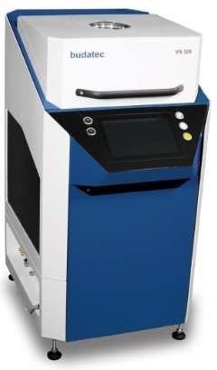
Designed specifically for handling high-force test assignments and accommodating large active surface areas during semiconductor verification processes. It serves as a dependable platform for ruggedized industrial components.
Typically engineered to support high-reliability processing requirements for IGBT and heavy power modules.
Features an advanced SEMI S2 compliant safety cabinet configuration optimized with responsive integrated visual feedback systems.
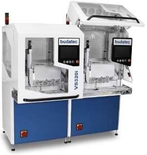
Equipped with a flexible multi-workholder positioning mechanism coupled alongside an agile 360° rotating head design.
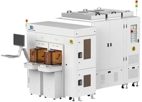
Engineered to deliver high-capacity automation paradigms directly to precision wafer-level verification routines. Built to ensure clean operation and damage-free manipulation.
Features automated cassette mapping matrices complemented by empty slot recognition to eliminate machine tracking errors.
Equipped with rigid, ultra-precise mechanical XY stages tracking across a generous 370 x 370 mm footprint.
A continuous high-yield inspection setup dedicated entirely toward executing high-reliability frame testing sequences.
Features automatic track width adjustment structures that swiftly conform to incoming production formats.
Utilizes intelligent processing architectures that execute automated wafer and strip map selection routines.
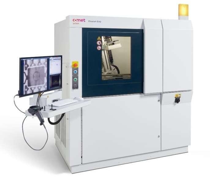
A non-destructive inspection unit engineered to grant three-dimensional structural insights into solder bumps within minutes.
Engineered with stable hardware modules designed to support continuous, highly precise, and reliable daily test routines.
Includes an intelligent software-assisted Dose Manager system aimed at shielding X-ray sensitive component modules during testing.
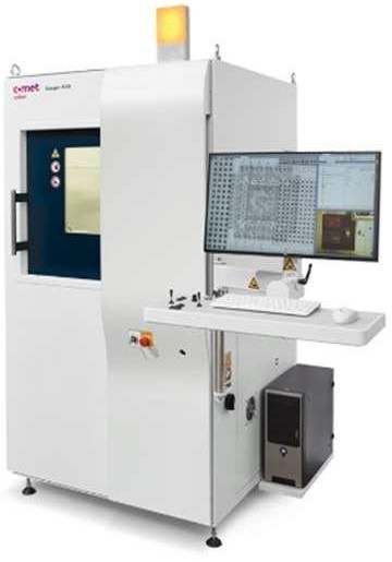
Advanced diagnostic platforms designed for both precision microfocus imaging and high-throughput production line inspection.
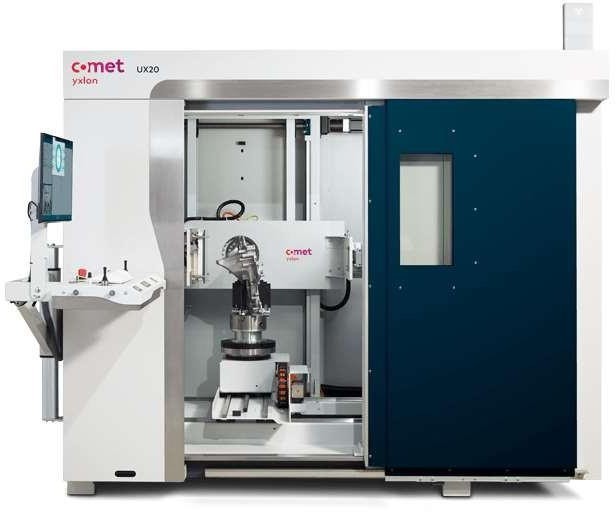
Advanced X-ray at CT inspection solutions para sa multi-material profiles at complex internal structural assemblies.
A high-precision inspection platform applied to locate sub-micron structural flaws across raw frames, wire paths, and semiconductor attachments.
Utilizes self-developed Absolute Precision Measuring hardware to monitor micro-fine shifting profiles along wire loops.
Employs deep neural networks trained via massive datasets to perform comprehensive defect filtering without missing outliers.
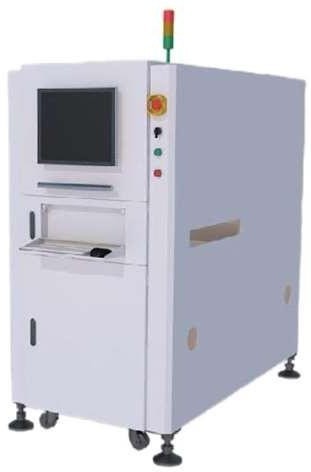
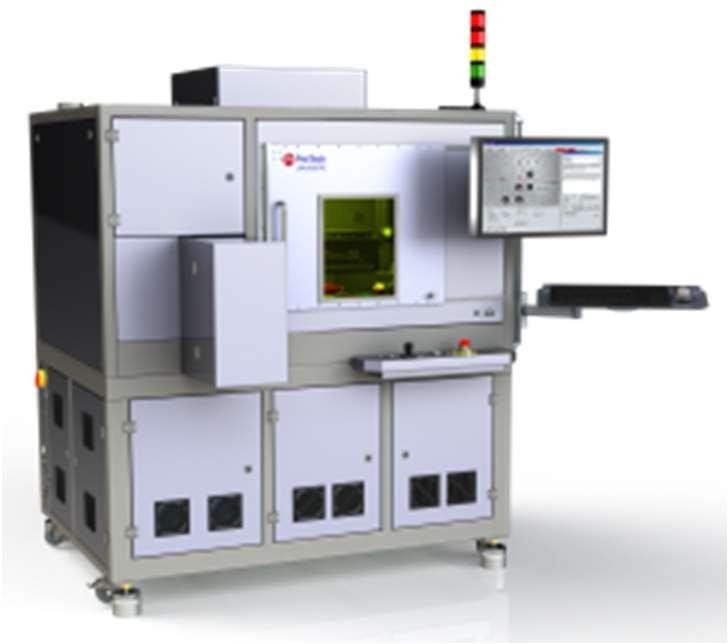
A targeted downstream automated optical detection rig designed to map structural flaws instantly after boards exit wave solder channels.
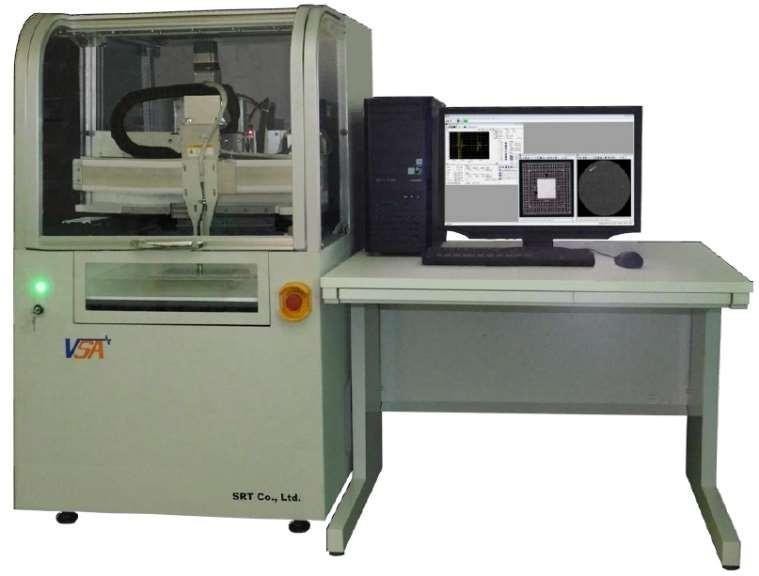
A high-end, micro-step substrate visual mapper focused entirely on scanning diced arrays and raw wafer profiles for microscopic defects.
An inline serialization processing solution geared to burn persistent tracking metrics, codes, and corporate branding onto electronic packages.
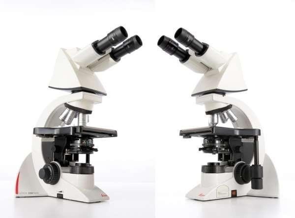
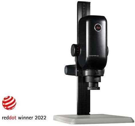
Comprehensive range of precision optical platforms for material analysis, component inspection, and digital documentation.
An all-in-one digital workspace solution designed to optimize robust streamlined inspections, measurements, and direct code-sharing tasks.
A critical metrology and automated processing electron microscope intended to deliver nanoscale imaging and dimensional calculation array mapping.
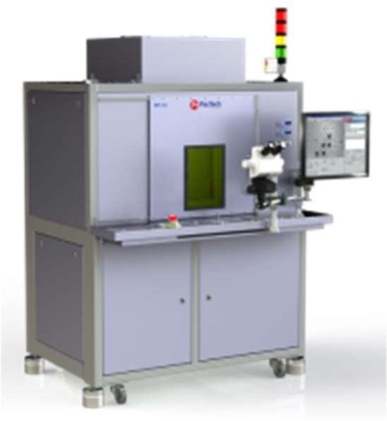
An innovative localized micro-ball jet placement processing system utilizing laser reflow methods for advanced electronic connectivity.
An advanced packaging machine designed to apply rapid, localized laser heating profiles to fine-pitch substrate configurations without mechanical or flux clean-up requirements.
A high-speed non-contact micro-particle removal deck utilizing shockwave air acoustics to strip target surfaces of loose debris without liquids.
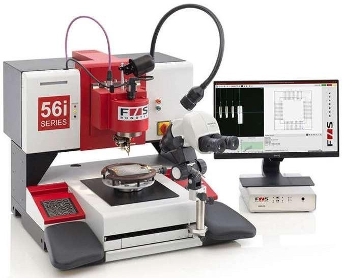
A flexible benchtop assembly platform capable of acting interchangeably as a high-precision wirebonder or an agile pull/shear testing platform.
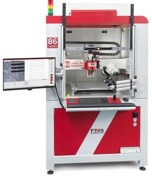
Provides optimized heavy-gauge tracking and large operational stages required for high-density automotive battery group bonding.
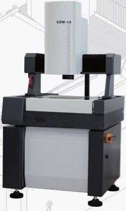
A high-end metrology tool tailored to extend structural dimension mapping tolerances using visual first-capture architectures.
An smart X-ray inspection cabinet configured to audit part inventory by instantly counting reeled SMD parts using neural algorithms.
A desktop scanning electron microscope featuring rapid vacuum pumping cycles to execute accelerated structural material analytics.
An ultra-high resolution laboratory x-ray testing unit integrating precise multi-axis positioning mechanisms within a compact footprint.
A high-power magnification imaging platform engineered to check small-hole drilling precision across complex multilayer PCB layouts and dense BGA/QFN mounts.
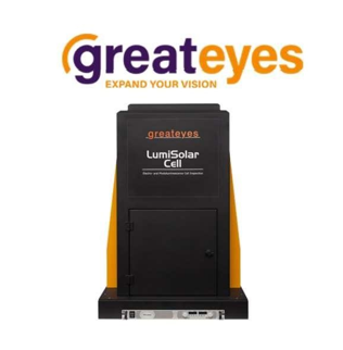
A multi-spectrum desktop diagnostics station combining electroluminescence, photoluminescence, and infrared testing for analyzing solar cell crystals.
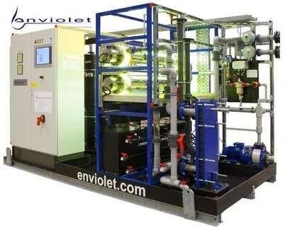
An industrial compact UV-oxidation fluid processing system engineered to execute large-scale disinfection workflows within advanced manufacturing environments.
An inline ultra-wide layout automated visual scanning deck processing heavy backplane panels in real-time.
A void-free thermal processing system utilizing deep closed-loop software control over isolated internal heating elements.
An automatic production line soldering platform integrated with multi-axis automated transport belts and optional formic acid cleaning systems.
| Equipment Category | Standard Features & Processing Scope |
|---|---|
| Precision Bond Testing | Forces spanning 1gf up to 1000kgf. Offers full 360-degree rotating tool heads, deep access reach (80mm), and nano-precise shear tracking heights. Includes automated cassette or frame handling links with SECS/GEM readiness. |
| X-Ray & Radioscopy Diagnostics | Sub-micron and nanometer defect detection pipelines. Automated void calculation powered by VoidInspect software extensions. Multi-axis manipulation with active Dose Management protection circuits. |
| Automated Optical Inspection (AOI) | 3D multi-focus visual mapping featuring infinite depth of field tracking. High-accuracy movement (±1μm) anchored onto ultra-dense stone platforms. Neural network systems running clean zero-negative sample filtration. |
| Microscopy & General Metrology | Upright, inverted, digital, and stereo optics platforms. High-speed sub-pixel calculation loops (0.2 sub-pixels accuracy) combined with rapid chamber pumping routines under 90 seconds. |
| Advanced Packaging & Thermal Prep | Fluxless, contact-free localized laser bonding matrices down to pitch profiles <80μm. Dry atmospheric or deep vacuum plasma surface activation systems. Void-free soldering ovens featuring Formic Acid integration options. |
We offer a wide range of reliable services including Risograph Printing, Customized Printing, Janitorial Supplies, Office Supplies, and ESD Products. Our goal is to deliver quality, efficiency, and cost-effective solutions tailored to your business needs.